Our investigations rely greatly on advanced optical experiments. We pay particular attention to building set-ups adapted to the exploration of the fabricated semiconductor nanostructures. Their goals are, on the one hand, to derive the fundamental features of the samples such as the optical losses, the photon or the carrier lifetimes and the thermal resistance. On the other hand, they are designed to demonstrate functions like laser emission or all optical switching, and to determine their performance. Our set-ups can be broadly divided as follows :
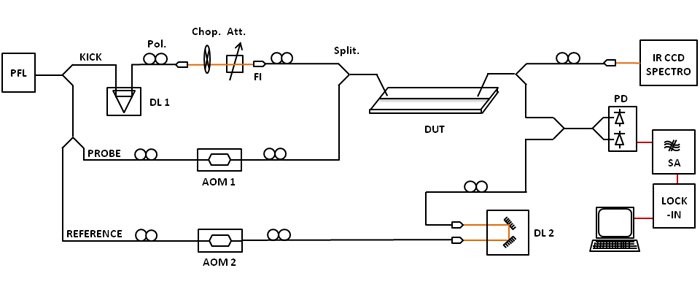
Pump-probe experiments are at the heart of the determination of the dynamics of physical effects such as a photo-induced refractive index change of a material. Their principle relies on the stimulation of the sample under investigation, with a powerful short optical pulse (100fs), the pump pulse and the probing of its characteristics at different time delay with a weak non perturbing pulse, the probe pulse.
Depending on the effects investigated, the detection is made either in the spectral domain using a spectrometer (non-degenerate pump probe) or directly in the time domain using heterodyne detection (degenerate pump probe). This type of set-ups allowed us lately the determination of the switching dynamics of our hybrid nanoswitch.

Pump-probe experimental set-up with heterodyne detection
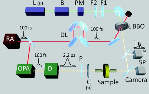
The accurate determination in the time domain of the optical signal propagating in nanostructures unveils without ambiguity many phenomena such as chromatic dispersion, gain switching in lasers or self-phase modulation in Kerr media. Our experiments are based on optical gating methods whose principle relies on instantaneous nonlinear wave mixing in a BBO crystal (Beta Barium Borate). Here, a high-intensity gate pulse provokes the frequency conversion of the signal arriving exactly at the same time. The frequency conversion taking place only during the coincidence with the gate pulse (within 100fs), the signal intensity can be precisely determined in the time domain by tuning the arrival time of the gate.

Optical gating experiment
Related publications:
Subduing surface recombination for continuous-wave operation of photonic crystal nanolasers integrated on Silicon waveguides
G. Crosnier, A. Bazin, V. Ardizzone, P. Monnier, R. Raj, F. Raineri, Opt. Express 23, 27953 (2015)
Ultrafast all-optical switching and error-free 10 Gbit/s wavelength conversion in hybrid InP-silicon on insulator nanocavities using surface quantum wells
A. Bazin, K. Lengle, M. Gay, P. Monnier, L. Bramerie, R. Braive, G. Beaudoin, I. Sagnes, R. Raj, F. Raineri, Appl. Phys. Lett. 104, 11102 (2014)
Temporal ringdown of silicon-on-insulator racetrack resonators
T. J. Karle, F. Raineri, V. Roppo, F. Bordas, P. Monnier, S. Ali, I. Sivan, R. Raj, Opt. Lett. 38, 2304 (2013)
Time-domain mapping of nonlinear pulse propagation in photonic-crystal slow-light waveguides
F. Raineri, T. J. Karle, V. Roppo, P. Monnier, R. Raj, Phys. Rev. A 87, 41802 (2013)
Dynamics of band-edge photonic crystal lasers
F. Raineri, A. Giacomotti, T. J. Karle, R. Hostein, R. Braive, A. Beveratos, I. Sagnes, R. Raj, Optics Express 17, 3165 (2009)