Involved People: Francesco Manegatti (PhD), Dimitris FITSIOS (Postdoc), Fabrice RAINERI (PI)
As photonic integrated circuits become more and more complex, with increased number of components, the need for power preservation becomes imminent. However, solutions for integrated optical amplification on Silicon substrates has not kept up with modern integration techniques, resulting in semiconductor optical amplifier solutions with huge footprint and power consumption values.
To overcome this, we aim to explore photonic crystal waveguide-based structures, based on III-V semiconductor materials integrated on SOI substrates. We take advantage of our established heterogeneous integration platform, which enables direct control over optical coupling between the silicon and III-V nanoamplifier levels. This leads to smooth interchange of light and prevent any catastrophic reflection feedback. The ultra-tight confinement of light offered by the photonic crystal structure guarantees for an increased confinement and gain factors. Our approach combines very small footprint and low power consumption values in a thin semiconductor membrane capable for integration with CMOS electronics. Finally, our proven electrical injection scheme can provide a compact, simple and efficient solution for the operation of nanoamplifiers in a fully functional complex photonic structures anywhere on the chip. A graphical representation of our coupling scheme, as well as an integrated array of nanoamplifiers can be seen in the Figures below.
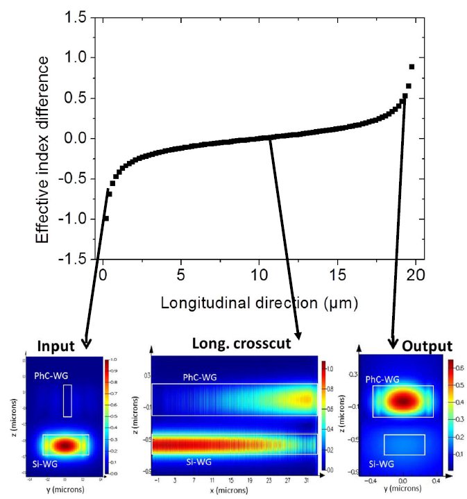
Calculations of the coupling scheme between the III-V photonic crystal waveguide and the SOI wire.
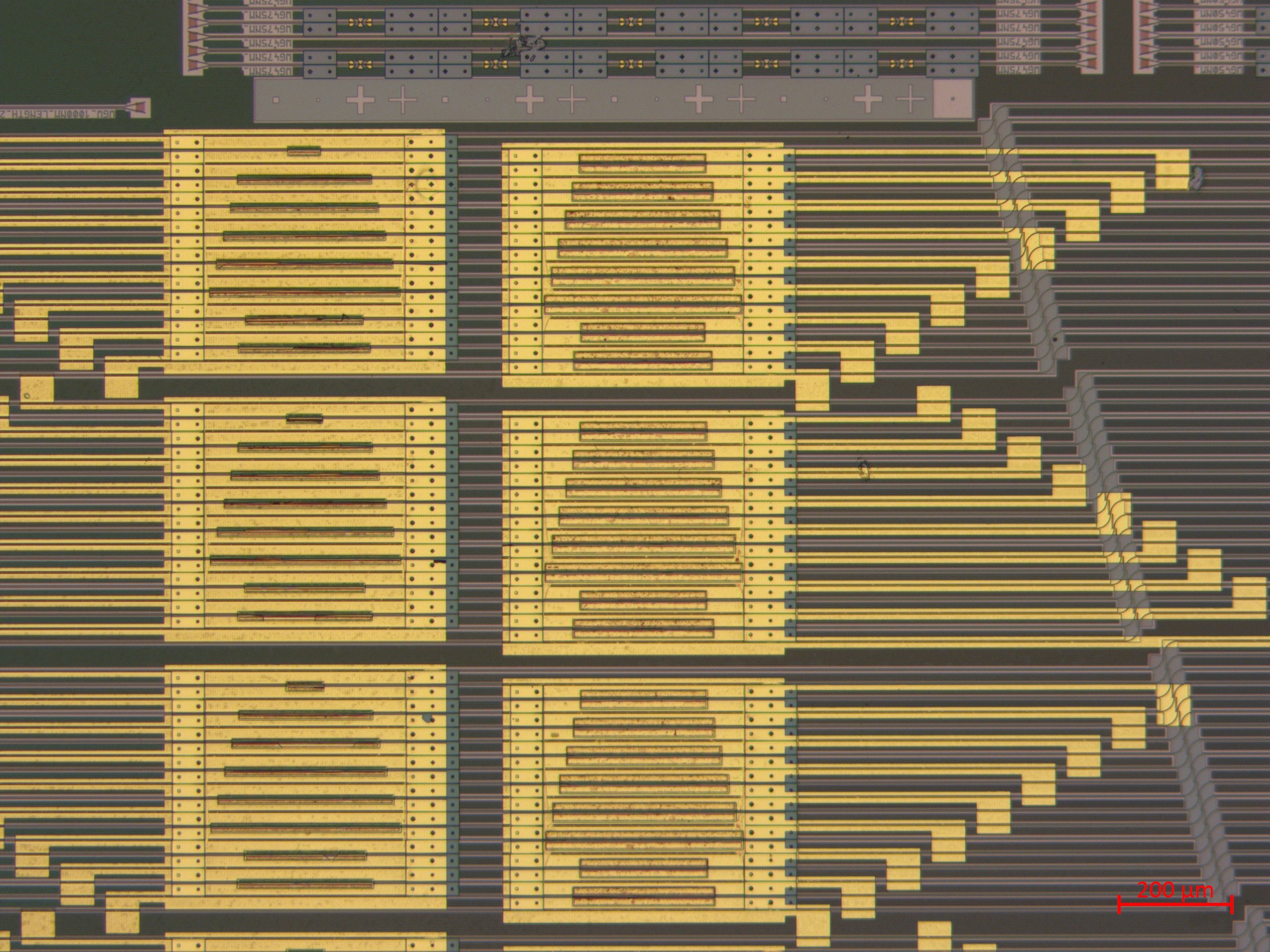
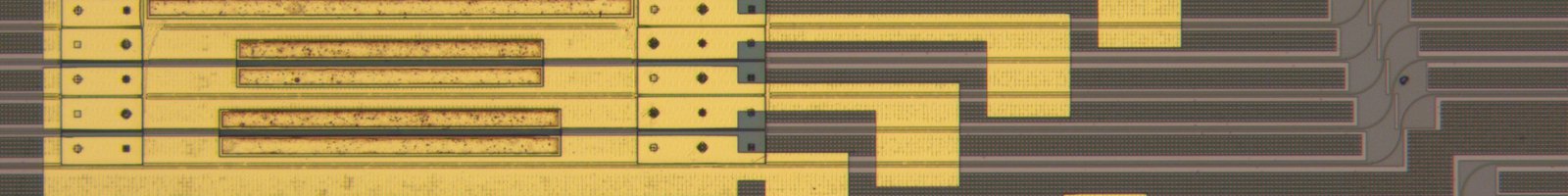
Optical microscope image of a fabricated nano-amplifier array.
Methods
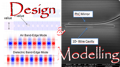
Our team follows a methodological approach based on the tackling of the challenges to be taken up in the 3 fronts which are the design and modelling", the material growth and nanoprocessing, and the experimental assesments. To know more, click on the images.
Fundings:
 H2020 RIA European project (2016-2019)