In this work, the concept of hybrid III-V semiconductor/silicon photonics was brought forward to nanophotonics by the integration of InP-based photonic crystal (PhC) nanolasers on Silicon on insulator single mode waveguides (see Fig. a) and b)). We demonstrated the most compact lasers integrated on a Si optical circuits with low thresholds and within the telecom window. This system has many assets in terms of performance and for future applications. Indeed, taking advantage of the quasi perfect confinement of light within PhCs, we fabricated lasers with 5µm² footprints which correspond to at least an order of magnitude reduction over previously demonstrated hybrid systems. The breakthrough result in this work is that almost all the emitted light is useful as it is efficiently coupled into the subjacent Si waveguides and thus can be further used directly in a CMOS compatible dense nanophotonic networks of interconnects adapted for computer-com. The highly efficient evanescent wave coupling was obtained by tailoring the optical properties of both the SOI waveguide and the III-V nanocavity and through the fine control over the technological processing of the structure such as the precise lithographic positioning of the nanocavity with respect to the SOI wires (Fig. c) and d)). Until now, the practical use of PhCs in an integrated photonic circuit has been an extremely challenging task. Establishing the communication between active nanodevices and the outside world, whilst mastering optical losses and photonic functionalities has been a major problem.
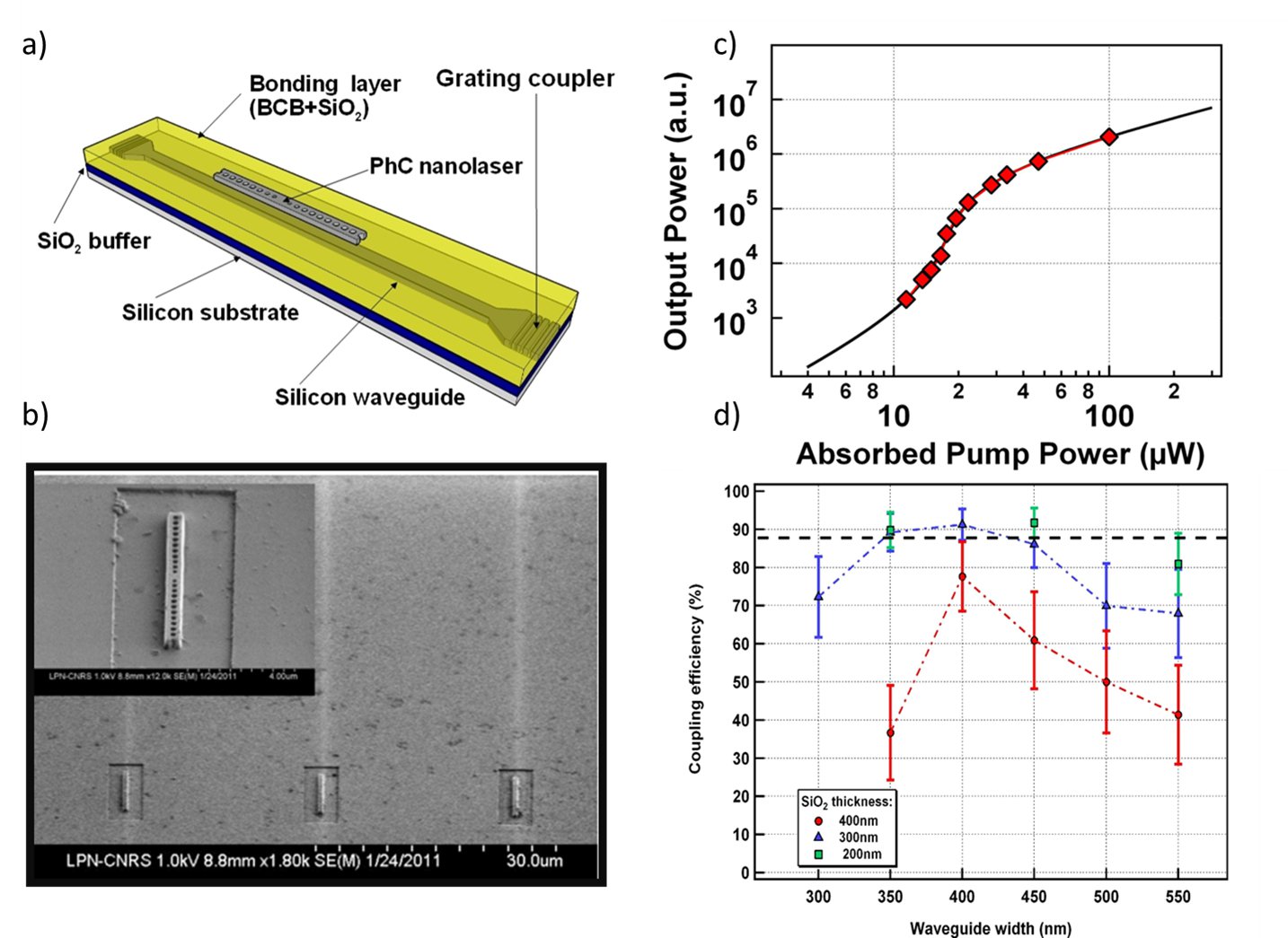
a) 3D schematical view of the hybrid structure. b) Scaning electron microscope top view of our fabricatednanolasers. c) Characteristic light-light curve of an hybrid nanolaser emitting at 1.55µm.d) Coupling efficiency of the emitted light into the SOI wire as a function of the structure parameters. We indicate by the black dotted line the estimated boundary in terms of coupling efficiency between lasing and non lasing structures.
The III-V/SOI hybrid system reported here brings an efficient and elegant solution for making use of active PhCs within a photonic circuit combining the best of III-V semiconductor and Si photonics.